Flexible printed electronics to help space missions lose weight
Tekniker is leading a European Space Agency (ESA) project to implement the development, manufacturing, testing and validation of printed structural electronics for use in space.
 The ability to integrate printed circuit boards and electronic assemblies directly into mechanisms and structures thanks to printing and thermoforming technologies opens up a range of possibilities in different sectors, such as household appliances and the automotive industry, where their use has begun to spread to car instrument panels, for example.
These new solutions are rapidly changing the way in which electronic functionalities are manufactured and integrated into any type of instrument or component, and are the ones that will be tested for the first time in Europe for space applications in a new project funded by the European Space Agency (ESA) led by the Basque technology centre Tekniker.
The main challenge of the Printed Structural Electronics (SIPRES) initiative will be to develop, manufacture and validate the use of flexible, printed and hybrid electronics with different prototypes that are capable of operating correctly in the extreme conditions of temperature, vacuum and radiation required by space exploration and research missions.
“This project is innovative because it marks the first time ESA will experiment with the application of printed electronics in flexible materials for use in space,” explains Borja Pozo, coordinator of Tekniker’s Space Sector.
“The weight of the devices and elements that are sent into space is a key and determining factor for the success of space missions. This technology, thanks to its lower material usage and reduced weight, can make future missions cheaper and more sustainable. It opens the door to integrating electronic capabilities more easily into multiple components and surfaces regardless of their shape,’ he adds.
Prototyping
Tekniker will contribute its knowledge and experience in electronics, manufacturing, surface chemistry and coating technologies throughout the development of the prototypes, from their conception phase to a technological development closer to their introduction into the space sector.
The process will also involve the engineering companies ALTER TECHNOLOGY and CT Ingenieros – Cadtech and will include the testing and validation of different polymeric materials, conductive inks and adhesives and manufacturing processes to resolve their compatibility with the required environmental conditions and space electronic components.
The printing of the electronic devices and assemblies will be carried out in Tekniker’s 3D printing laboratory.
Once developed, tested and validated, the first technology demonstrators could be implemented with nanosatellite platforms commonly used for low Earth orbit (LEO) research or in the verification of the International Space Station (ISS) test campaign.
In parallel, based on the roadmap established by ESA, the application of the final prototypes for future missions to the Moon and Mars could be considered.
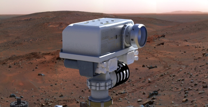
“Among the possible solutions that could be developed with this technology are the integration of wind and humidity sensors for Mars rovers; radiation, temperature and photodetector sensors for the Moon; force sensors for spacecraft mechanisms; or solar and thermal energy systems for small low-orbit satellites,’ adds the Tekniker expert.
These solutions also open up possibilities for online telemetry supervision, i.e. for remote real-time monitoring and data transmission.
The SIPRES initiative, which will start this October and run for two years, is funded by ESA as part of its TDE technology development programme.
Tekniker has collaborated and continues to collaborate with ESA through various projects, including testing the effects of the space environment on materials and investigating new ways to generate fuel for space missions.